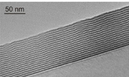
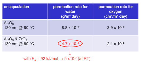
91ÖÆƬ³§

Encapsulation

Encapsulation

Al2O3 / ZrO2 nano laminate film for OLEDs Ref: Meyer, J. et al. Appl Phys Lett 94, 233305 (2009).

Encapsulation and barrier layers are one of the most striking success stories of ALD and are now used in production to fulfill stringent applications such as OLED or flexible electronics. ALD can deliver uniquely dense pinhole-free films making it the technique of choice to obtain high-quality ultra-thin moisture barrier layers and anti-oxidation films. The ability to deposit nanolaminate films with atomic-level thickness control enables to achieve excellent permeation performances with water transmission rates below 1E-6 g/m2/ day while ALD superior conformallity will provide full coverage even over complex 3D nano- and micro-structures, making it highly suitable for MEMS / NEMS applications. The film properties can also be tuned to ensure that it remains optically transparent and clear to the eye making it attractive to protectively coat precious metals and artifacts.

THIN FILM ENCAPSULATION

91ÖÆƬ³§Cambridge Nanotech has been at the forefront of the development of ALD films for encapsulation and barrier layers. Pioneering works from Carcia and Meyer on Savannah® ALD platforms have demonstrated the potential of ALD to fulfill the most stringent encapsulation requirement with water transmission rates below 1E-6g/m2/day. Our scientists have years of experience in the development of hybrid organic / inorganic films deposited by MLD (Molecular Layer Deposition) integrating organic layers such as alucone or zircone in an inorganic oxide matrix. Such hybrid materials can provide more flexible films while still ensuring superior impermeability.

The low thermal budget and ultra thin nature of these films has proved critical for the most stringent applications such as OLEDs or flexible electronics applications on organic substrates such as PEN or PET.

Encapsulation by ALD can also provide excellent oxidation barrier on metals and has been successfully used to protect coins, artifacts and other oxidation-sensitive materials.

ALD Benefits for Encapsulation

  • Atomic thickness control and conformallity
    Deposit sub-µm nanolaminate oxides with superior uniformity and conformality even over complex 3D nano-structures
  • Dense pinhole-free films
    To achieve thin films with WVTR below 1E-6 g/m2/day
  • Low thermal budget
    ALD films can be deposited below 100ËšC suitable for organic electronic applications
  • Production-ready
    The films you developed in R&D are readily scalable for production

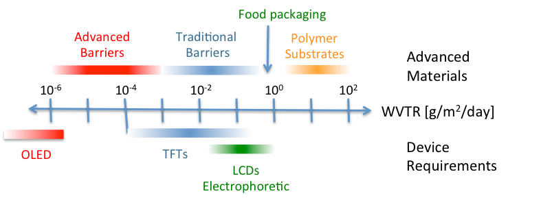
ALD thin films can provide optimal moisture barriers films to satisfy the most stringent applications such as OLEDs with water vapor transmission rate below 1E-6 g/m2/day for films thinner than 50 nm.

Ref: Advanced Materials 2009, 21, 1845-1849

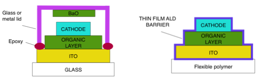
Advanced thin films barriers are required for MEMS and OLED packaging. ALD can deliver ultra-thin encapsulation with superior conformallity and thickness control making it the technique of choice for flexible electronics.

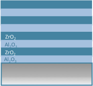
ALD enables to deposit multi-component nanolaminate oxides to combine Al2O3 excellent moisture barrier performance with the anti-corrosion properties of alternative oxides such as HfO2, ZrO2 or SiO2 in aqueous environments.

Nanolaminate oxide deposited at 80˚C in Savannah® as an encapsulation for low cost OLEDs.

  1. Meyer, J., et al. (2009) Applied Physics Letters, 94(23), 233305
  2. Meyer, J., et al. (2009) Advanced Materials, 21(18), 1845–1849

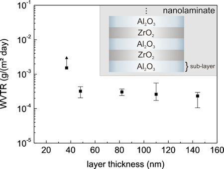
Impact of layer thickness on Water Vapor Transmission Rate (WVTR). WVTR at 3.2E-4 g/m2/day at 80ËšC for 40 nm film corresponds to 8.7E-7 g/m2/day at room temperature.

Ref: Meyer, J., et al. Applied Physics Letters, 96, 243308 (2010).

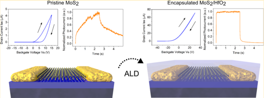
Encapsulation by ALD can be employed in a broad range of applications. In the above example, HfO2 is used to protect a 2D MoS2-based sensor from the environment while maintaining the device record responsivity and sensitivity.

Ref: Kufer, D. & Konstantatos, G.. Nano Lett 15, 7307–7313 (2015).

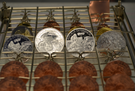
ALD is ideal to provide cost-effective anti-tarnish coatings on precious metals and artifacts. This technique can be readily scaled up to meet your production requirement in a cost effective solution.

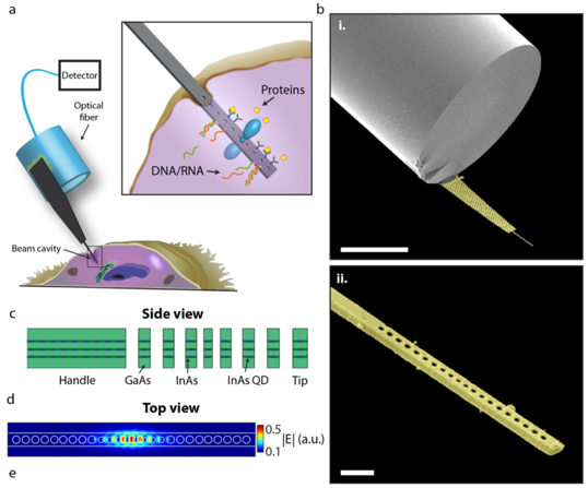
A 7-10 nm Al2O3/ ZrO2 nanolaminate is deposited on a GaAs photoluminescent nanocavity probe. The device is used to probe a single cell and the ALD nanolaminate prevents the photo-induced oxidation in the aqueous media without altering the device response.

Shambat, G. et al. Single-cell Photonic Nanocavity Probes. Nano Lett 130206113907001 (2013)

View publication review on Encapsulation Films done in 91ÖÆƬ³§CNT platforms


REFERENCES – Recent publications done on 91ÖÆƬ³§CNT ALD platforms

  1. Wegler, B., et al., (2014). Influence of PEDOT:PSS on the effectiveness of barrier layers prepared by atomic layer deposition in organic light emitting diodes. JVST A, 33(1), 01A147.
  2. Warnat, S., Forbrigger, C., Hubbard, T., Bertuch, A., & Sundaram, G. (2014). Thermal MEMS actuator operation in aqueous media/seawater: Performance enhancement through atomic layer deposition post processing of PolyMUMPs devices. JVST A, 33(1), 01A126. doi:10.1116/1.4902081
  3. Carcia, P. F, et al.,. (2013). Effect of early stage growth on moisture permeation of thin-film Al2O3 grown by atomic layer deposition on polymers. JVST A, 31(6), 061507. doi:10.1116/1.4816948
  4. Clark, M. D., et al., Ultra-thin alumina layer encapsulation of bulk heterojunction organic photovoltaics for enhanced device lifetime. Organic Electronics, 15(1), 1–8. doi:10.1016/j.orgel.2013.10.014
  5. Carcia, P. F., et al. (2012). Permeability and corrosion in ZrO2/Al2O3 nanolaminate and Al2O3 thin films grown by atomic layer deposition on polymers. JVSTA, 30(4), 041515–041515–5. doi:10.1116/1.4729447
  6. Carcia, P. F., McLean, R. S., Sauer, B. B., & Reilly, M. H. (2011). Atomic Layer Deposition Ultra-Barriers for Electronic Applications—Strategies and Implementation, 11(9), 7994–7998. doi:10.1166/jnn.2011.5075
  7. Chang, C.-Y., & Tsai, F.-Y. (2011). Efficient and air-stable plastics-based polymer solar cells enabled by atomic layer deposition. Journal of Materials Chemistry, 21(15), 5710. doi:10.1039/c0jm04066e
  8. Carcia, P. F., et al. (2010). Encapsulation of Cu(InGa)Se2 solar cell with Al2O3 thin-film moisture barrier grown by atomic layer deposition. Solar Energy Materials and Solar Cells, 94(12), 2375–2378. doi:10.1016/j.solmat.2010.08.021
  9. Carcia, P. F., et al. (2010). Permeation measurements and modeling of highly defective Al2O3 thin films grown by atomic layer deposition on polymers. Applied Physics Letters, 97(22), 221901. doi:10.1063/1.3519476
  10. Meyer, J., and al., (2010).The origin of low water vapor transmission rates through Al2O3/ZrO2 nanolaminate gas-diffusion barriers grown by atomic layer deposition. Applied Physics Letters, 96(24), 243308–243308–3.
  11. Sarkar, S., et al., (2010). Encapsulation of organic solar cells with ultrathin barrier layers deposited by ozone-based atomic layer deposition. Organic Electronics, 11(12), 1896–1900. doi:10.1016/j.orgel.2010.08.020
  12. Meyer, J., et al., (2009). Al2O3/ZrO2 Nanolaminates as Ultrahigh Gas-Diffusion Barriers-A Strategy for Reliable Encapsulation of Organic Electronics. Advanced Materials, 21(18), 1845–1849. doi:10.1002/adma.200803440
  13. Meyer, J., et al. (2009). P-157: Highly-Efficient Gas Diffusion Barriers Based on Nanolaminates Prepared by Low-Temperature ALD. SID Symposium Digest of Technical Papers, 40(1), 1706. doi:10.1889/1.3256661
  14. Meyer, J., et al. (2009c). Reliable thin film encapsulation for organic light emitting diodes grown by low-temperature atomic layer deposition. Applied Physics Letters, 94(23), 233305. doi:10.1063/1.3153123
  15. Chang, C.-Y., et al., Thin-film encapsulation of polymer-based bulk-heterojunction photovoltaic cells by atomic layer deposition. Organic Electronics, 10(7), 1300–1306. doi:10.1016/j.orgel.2009.07.008
  16. Görrn, P., Riedl, T., & Kowalsky, W. (2009). Encapsulation of Zinc Tin Oxide Based Thin Film Transistors. The Journal of Physical Chemistry C, 113(25), 11126–11130. doi:10.1021/jp9018487
  17. Kim, N. (2009). Fabrication and characterization of thin-film encapsulation for organic electronics. PhD Dissertation, Georgia Tech – http://hdl.handle.net/1853/31772
  18. Kim, N., et al., (2009). A hybrid encapsulation method for organic electronics. Applied Physics Letters, 94(16), 163308. doi:10.1063/1.3115144
  19. Potscavage, W. J., Yoo, S., Domercq, B., & Kippelen, B., (2007). Encapsulation of pentacene/C60 organic solar cells with Al2O3 deposited by atomic layer deposition. Applied Physics Letters, 90(25), 253511. doi:10.1063/1.2751108