Atomic Layer Deposition (ALD) offers precise control down to the atomic scale.Atomic layer deposition holds tremendous promise across a wide array of industries, including energy, optical, electronics, nanostructures, biomedical, and more. Please check out our Applications section for more details in any and all of these areas.
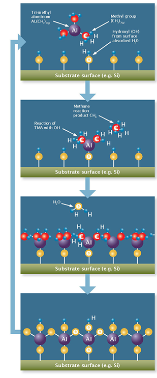
The principle of atomic layer deposition is similar to chemical vapor deposition (CVD) except the ALD reaction breaks the CVD reaction into two half-reactions, keeping the precursor materials separate during the reaction.
This is accomplished through sequential pulsing of special precursor vapors, each of which forms about one atomic layer during each pulse (reaction cycle). Reaction cycles are then repeated until the desired film thickness is achieved, versus chemical vapor deposition that introduces multiple precursor materials simultaneously.
Our atomic layer deposition systems (���������ԲԲ���®, ���ᾱ® and Phoenix® Firebird™) are designed to deposit pinhole free coatings that are perfectly uniform in thickness, even deep inside pores, trenches and cavities.
The ability to deposit such high quality films on substrates with ultra-high aspect ratios is a key feature of our atomic layer deposition systems.
A wide variety of thin films can be deposited using gas, liquid, or solid precursors.
Please see a list of materials that are commonly used in our ALD materials section.
Contact us if you are interested in learning how we simplified ALD while making it accessible and within financial reach for researchers.