Atomic layer deposition has been around for decades but it was the efforts to integrate ALD high-k materials as a gate dielectric in logic devices and a capacitor dielectric in DRAM that inspired the research community to master the technique and expand its range of uses.
Veeco/CNT ALD systems have been used to study a variety of high-k dielectric materials including Al2O3, HfO2, Ta2O5, TiO2, and ZrO2. The flexibility of the ALD technique allows for tweaking of film properties through combination of films, ie AlTiO, HfSiO, etc., or through the incorporation of nitrogen in such films as AlON, HfON, and ZrON. ALD high-k dielectric film properties include high capacitance, low leakage current, and high breakdown voltage making them suitable for electronics applications.
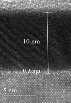
HRTEM of nitrided HfO2 deposited on Fiji®. L-T Huang, et al. “Improvement in electrical characteristics of HfO2 gate dielectrics treated by remote NH3 plasma,” Applied Surface Science Volume 266, 1 February 2013, Pages 89-93.
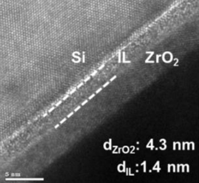
HRTEM of Fiji® deposited ZrO2 on nitrided Al2O3 buffer layer. J-J Huang, et al. “Improvement in Electrical Characteristics of Crystalline ZrO2 /Nitrided Al2O3 Gate Stacks Grown by Remote Plasma Atomic Layer Deposition,” ECS J. Solid State Sci. Technol. 2013 volume 2, issue 12, P524-P528
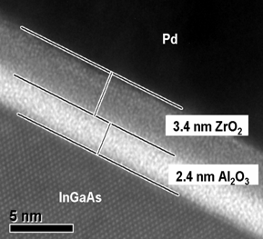
HRTEM of Fiji® deposited ZrO2/Al2O3 stack. A. O’Mahoney, et al. “Structural and Electrical Analysis of Thin Interface Control Layers of MgO or Al2O3 Deposited by Atomic Layer Deposition and Incorporated at the high-k/III-V Interface of MO2/InxGa1-xAs (M = Hf|Zr, x = 0|0.53) Gate Stacks,” ECS Transactions, 33 (2) 69-82 (2010).
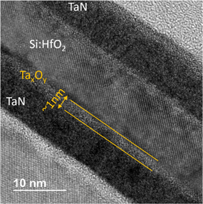
HRTEM of Fiji® deposited Si:HfO2 film. P.D. Lomenzo, et al. “TaN interface properties and electric field cycling effects on ferroelectric Si-doped HfO2 thin films,” Journal of Applied Physics 117, 134105 (2015).
With major logic and memory chip makers integrating high-k ALD films into their products, the ALD technique gained acceptance in the fab and the search was on for other device regions where ALD films could provide disruptive gains in performance and cost.
Electrodes
Materials for device electrodes must have appropriate properties. Low-resistivity is a primary concern but other film properties including appropriate work function and chemical compatibility with other device materials are essential. ALD can produce a range of pure metals (Pt, Ru, Ni) as well as metal nitrides (TiN), and conducting oxides (RuO2) which have all been investigated as electrode materials in electronic applications.
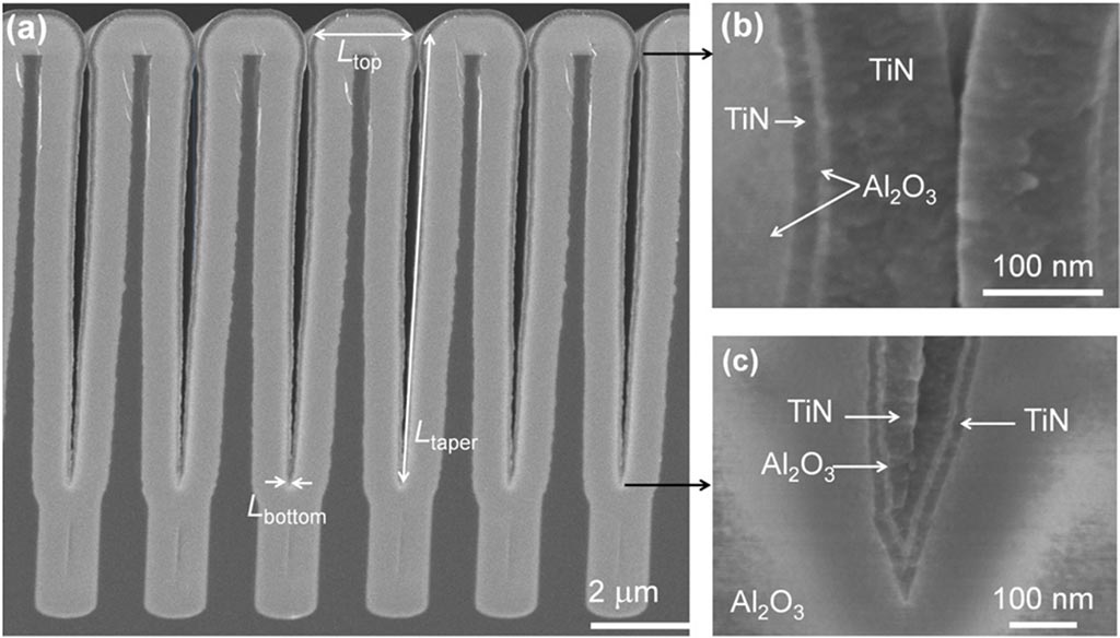
Cross-section SEM images of Fiji® deposited TiN-Al2O3-TiN trench capacitors. M. Burke, et al. “High aspect ratio iridescent three-dimensional metal–insulator–metal capacitors using atomic layer deposition,” J. Vac. Sci. Technol. A 33(1), Jan/Feb 2015.
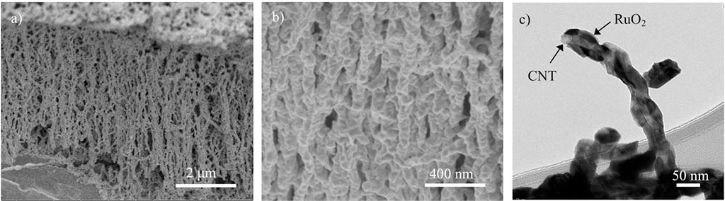
a) and b) SEM images of Fiji® deposited RuO2 coated carbon nanotubes and c) TEM of single RuO2 coated carbon nanotube. R. Warren, et al. “ALD Ruthenium oxide-carbon nanotube electrodes for supercapacitor applications,” 2014 IEEE 27th International Conference on Micro Electro Mechanical Systems (MEMS).
Barriers
Modern integrated circuits utilize nanoscale, multilayer wiring schemes to interconnect the discrete devices on the semiconductor substrate to produce useful circuits, provide power distribution, and as input/output pathways for off-chip communications. These interconnects are typically fine copper lines which have been deposited onto patterned low-k interlayer dielectric (ILD) materials which support and define the connection pathways. Copper is a highly mobile material and if deposited directly on the ILD, will diffuse into the dielectric and device performance will degrade over time.
Barrier films are necessarily deposited on the ILD prior to copper deposition. The thinner and more conductive the barrier film is, the less overall impact it will have on the interconnect resistance. ALD is particularly suited for barrier applications with its ability to deposit thin, conformal, pinhole free, and highly conductive films with very low copper diffusion characteristics. Numerous ALD nitride processes have been developed on Veeco/Cambridge NanoTech systems.
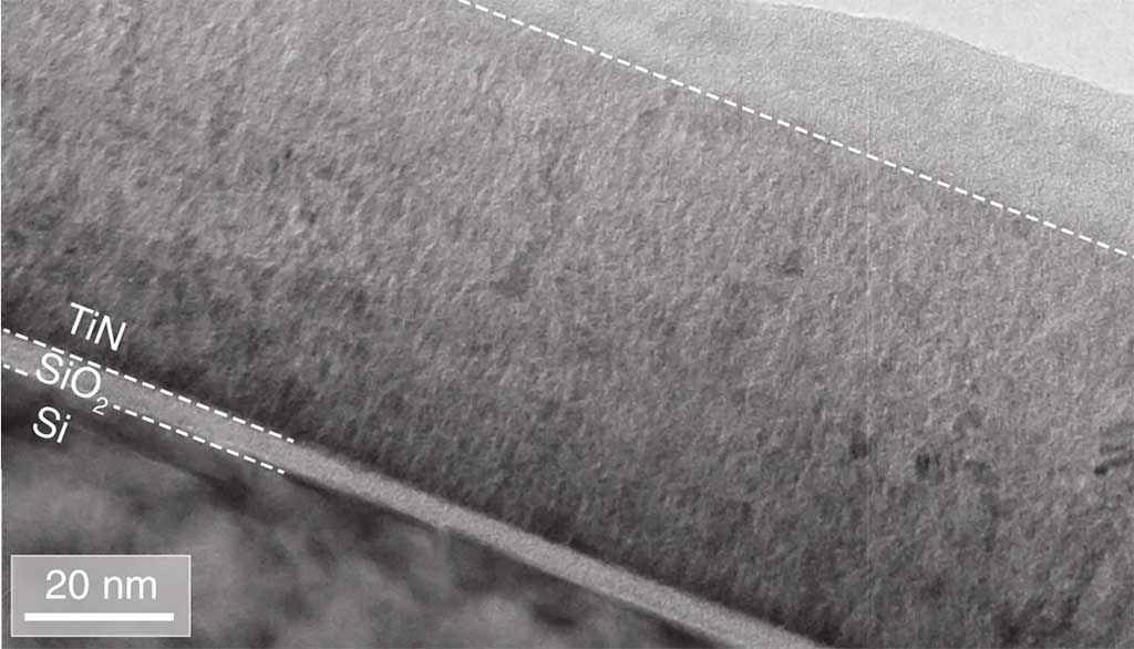
TEM image of Fiji® deposited TiN. L. Assaud, et al. “Highly-Conformal TiN Thin Films Grown by Thermal and Plasma-Enhanced Atomic Layer Deposition,” ECS Journal of Solid State Science and Technology, 3 (7) P253-P258 (2014).