Chalcogenides—compounds made from elements like sulfur, selenium, or tellurium mixed with metals—are gaining traction across the tech world. Why? Because they can quickly and reliably switch states and control how light or heat moves through a material. That makes them incredibly valuable for data storage, optical systems, and energy devices where performance, speed, and efficiency are vital. Chalcogenide materials consist of at least one chalcogen anion (group 16 element), in particular sulfide, selenide, and telluride, shown in red. The transition metals chalcogenides consist of a transition metal (d-block elements) bonded with a chalcogenide (S, Se, Te). These materials exhibit unique material properties and are highly covalent, exhibiting semiconducting properties.
Transition metal dichalcogenides (TMD) include metals that form a metal disulfide (MS2), metal diselenide (MSe2), or metal ditelluride (MTe2). TMD materials of particular interest in recent research are shown in green on the periodic table.
They can switch between amorphous and crystalline states: perfect for fast, reversible data storage like phase-change memory. They also offer tunable optical properties for reconfigurable lenses, and in thermoelectric devices, they help manage heat and generate power.
To make it all work, precision matters. Techniques like ALD and sputtering apply thin, even layers. Post-deposition annealing controls the switching behavior, and smart interface design keeps multilayer devices running smoothly.
You’ll find chalcogenides at the heart of:
91��Ƭ��provides the tools that make working with these materials possible. Our systems offer atomic-scale film control, real-time monitoring, and the scalability needed to move from R&D to full production, without sacrificing precision.
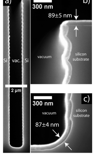
Atomic layer deposition techniques can be used to deposit thin film chalcogenide materials, either directly, or by utilizing a sulfurization anneal after the ALD deposition. ALD techniques offer unique capabilities to deposit films on three dimensional features in a conformal manner with accurate material composition and controlled film thickness.
There has been a pronounced interest in transition metal chalcogenide materials for photovoltaics, photonics, catalysis, and energy storage applications. Of particular interest have been the sulfide chalcogenide materials.
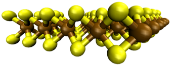
Examples of chalcogenide films deposited on CNT platforms
Ref: Dasgupta, N. P., et al., Accounts Chem Res 48, 341–348 (2015).
CHALCOGENIDE PHOTOVOLTAICS
Atomic layer deposition techniques can be used to deposit thin film chalcogenide materials.
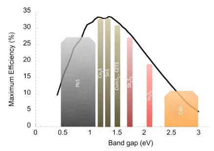
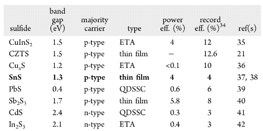
Chalcogenide materials for photovoltaics applications have been explored for the absorber materials where bandgap energies are better suited to achieve higher levels of efficiency ( 31 – 34% efficiency at 1-1.6 eV). Quaternary films can be deposited using ALD techniques, including copper zinc tin sulfide (CZTS). ALD deposited materials can also be used for fabricated buffer / emitter materials (In2S3, ZnS, CdS, and Zn(O,S)).
ENERGY STORAGE
ALD deposited films have been investigated in energy storage and battery applications with demonstrated levels of improved performance.
PHOTONICS
Chalcogenide materials have also been used in the photonic and solar applications.
ZnS for TFEL displays (first ALD industrial application)
2D DICHALCOGENIDES
Two dimension dichalcogenides have been investigated for their unique material properties, including band gap semi conducting properties, photoluminescence, and absorbance as the film thickness is reduced to one monolayer thickness. Atomic layer deposition offers a direct method toward achieving a one molecular layer thick film. Research is actively being pursued to develop a two step process utilizing ALD and a sulfurization anneal, or a direct growth method for transition metal dichalcogenide (TMD) materials.
ZnS for TFEL displays (first ALD industrial application)